
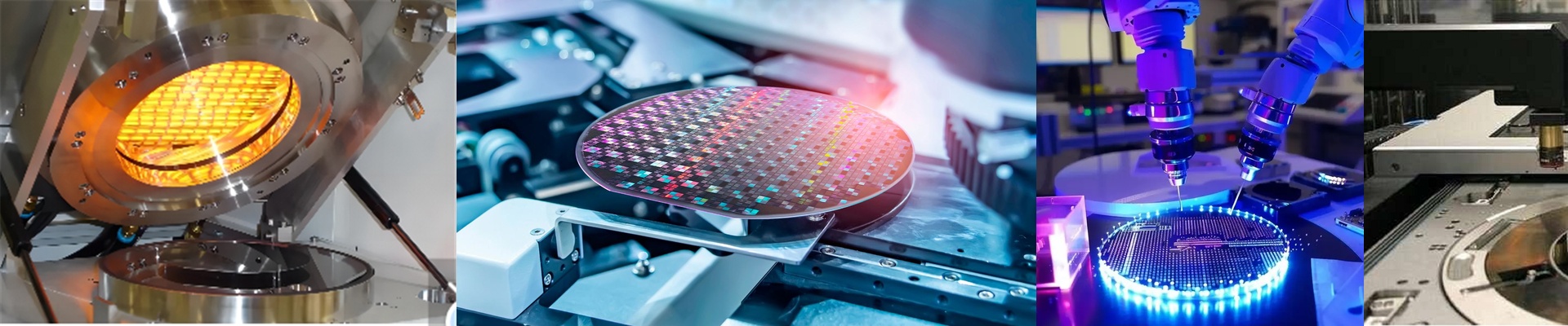
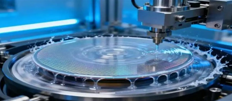
On the line, the clock doesn’t wait for thermal drift. In a 300 mm fab, underfill curing sits at the tail end—after bump, after flip-chip bonding—where throughput and yield are measured in seconds, and defects are measured in microns. Let the thermal profile drift and you’ll see voiding, fillet collapse, or CTE mismatch stress that shows up later as field failures. When the IR source underperforms, the oven stretches the dwell to compensate, and the line stops keeping pace. We built our semiconductor IR underfill curing around one hard requirement: process control that behaves like a spec, not a wish.
What matters, technically
IR underfill curing isn’t just heat—it’s repeatable heat, delivered on demand. We use near-infrared (NIR) emitters engineered for rapid, localized energy delivery, so you get fast ramp rates and short dwell times without overshoot. The system is designed to meet the thermal control expectations of semiconductor equipment: temperature stability and uniformity are specified, measured, and documented. Key thermal behavior is defined by:
- Wafer-level thermal uniformity: Specified to ±0.1°C across the active zone, verified with mapped thermocouple and pyrometer cross-checks.
- Photoresist bake compatibility: Soft bake and hard bake profiles can be held within tight tolerance, protecting critical dimensions in lithography stacks.
- Thermal repeatability: Run-to-run profiles match within a narrow band, so qualification doesn’t get re-done every shift.
- Cleanroom compatibility: Construction and exhaust routing support Class 1–100 environments, with materials and seals chosen to keep particle counts down.
- Zero particle generation: Internal airflow and hot-zone geometry minimize shedding, and surfaces are selected to avoid outgassing that can contaminate wafers. This hardware is specified like production equipment, not a benchtop heater: standard voltage options, defined mechanical envelopes, and connector compatibility that fits automated integration. Control is closed-loop, using calibrated sensors and a control strategy tuned for quick response and a stable steady state. Reliability is measured in uptime. The system runs 24/7 with scheduled maintenance windows, and unplanned downtime is minimized by modular emitter assemblies and predictable consumable replacement.
Why it works in this environment
Underfill curing in semiconductor packaging and advanced assembly is where thermal performance shows up on the yield sheet. You need a fast cure to keep the line moving, but you can’t trade speed for voids. With controlled NIR energy, the underfill cures quickly while maintaining a clean thermal front—reducing the risk of trapped volatiles and micro-void formation. The result is a stable fillet profile and consistent adhesion, which matters for reliability testing and for the next assembly steps. The same thermal control that supports underfill also supports upstream photoresist processing. When you run photoresist bake steps, temperature uniformity directly affects solvent removal and crosslinking. Non-uniformity shows up as linewidth variation and scumming after develop. Holding the bake profile within tight limits cuts CD dispersion and improves process capability. In practice, you get:
- Tighter process windows: Repeatable profiles reduce excursions and rework.
- Lower energy cost: Shorter dwell and localized heating cut the thermal load on the chamber and support systems.
- Fewer spares: Modular design and long emitter life reduce spare inventory and changeover time.
- More consistent output: Less drift means fewer line stops and fewer false alarms from SPC limits. This isn’t a repurposed thermal tool. It’s an underfill curing solution engineered to match the expectations of semiconductor equipment—thermal precision, clean operation, and sustained uptime.
Things to know before you roll it in
No thermal system is plug-and-play in a fab without planning. Installation needs attention in three spots:
- Utility alignment: Confirm voltage, amperage, and coolant routing to match the line’s infrastructure. The system is designed for standard fab power and cooling interfaces, but the site has to allocate capacity up front.
- Space and integration: The mechanical envelope and service access have to fit the tool layout. Plan for emitter replacement access and sensor calibration access.
- Exhaust and cleanroom discipline: Even with low outgassing materials, the exhaust path must be routed as specified to maintain cleanroom compliance and prevent recirculation. One trade-off is real: performance depends on emitter-to-substrate distance and field uniformity. If you change the substrate geometry or the fixture significantly, the thermal profile needs re-qualification. We provide mapping procedures and setpoint guidance, but process transfer to a new stack or fixture always requires a short qualification run. If you’re qualifying an alternative to an existing IR source, the validation path is straightforward. We supply mapped uniformity data, calibration curves, and repeatability reports in a format that lines up with your equipment acceptance protocols. The goal is a validated, equivalent thermal solution—one that meets the same performance targets as your current equipment, backed by documented evidence. When the line is running, the only acceptable temperature is the one you specified. Our underfill curing system for semiconductor IR is built to deliver it—every cycle.